EMCTrace Blog
PCB Design guidelines, layout reviews, and EMC fundamentals. Straight from our experts.
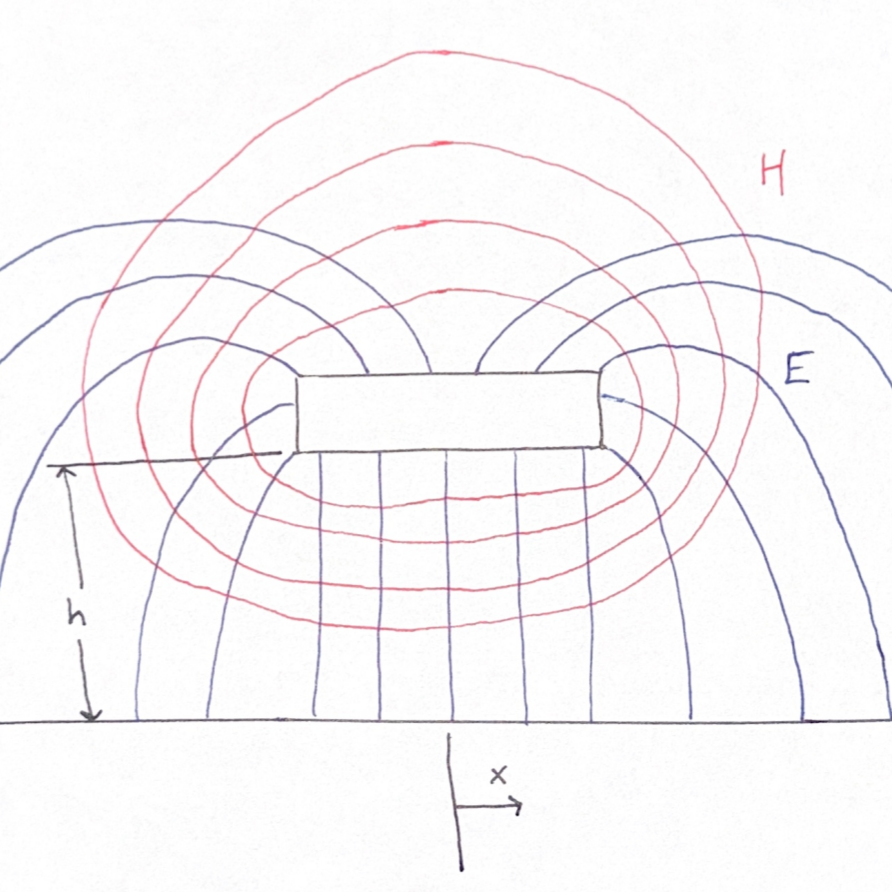
Field Spread in Microstrip Traces
What causes crosstalk and how to minimize field spread.
8/5/2026
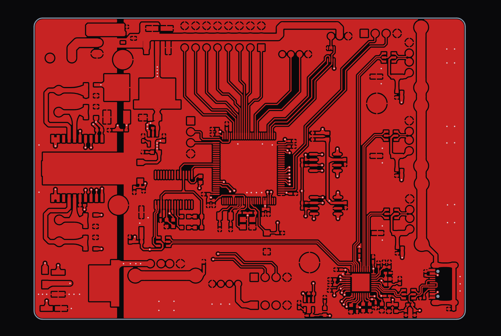
A Misuse of a SGPS 4-Layer Stackup
How to use SGPS boards, and how they can be improved for EMC performance.
7/21/2026
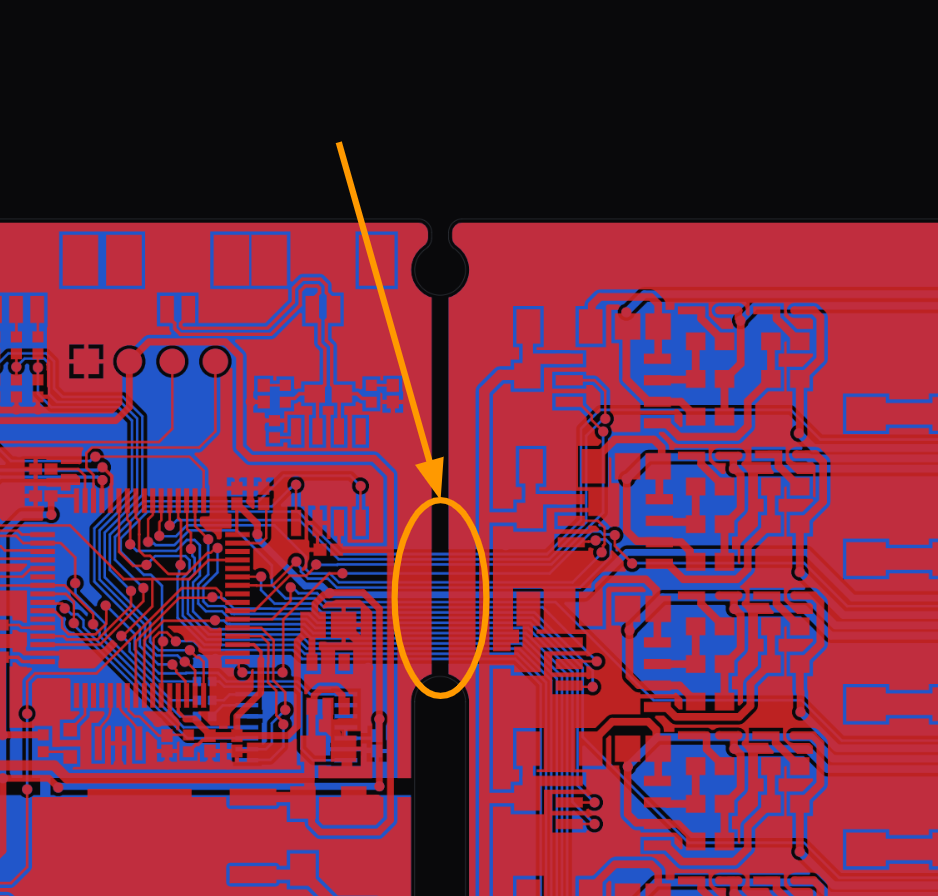
Crossing a Split in Reference Copper
An analysis of what happens when high-speed traces cross a gap in reference copper that extends to the board edge.
7/14/2026
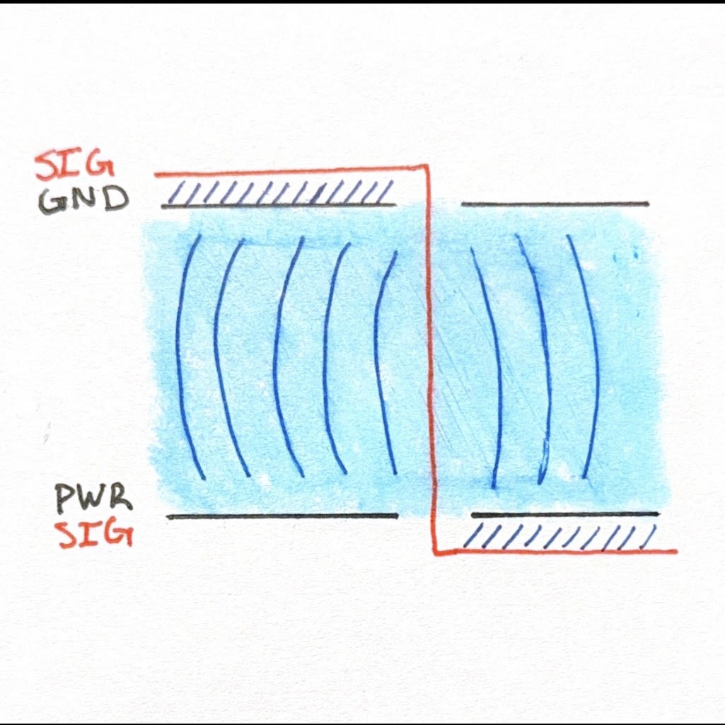
Managing Fields in an SGPS Stackup
How to avoid EMC risks when transitioning between layers with a 4-Layer SGPS PCB.
7/7/2026
How to Route Differential Pairs
A brief guide on the what to avoid and what to prioritize in differential pair routing.
6/30/2026
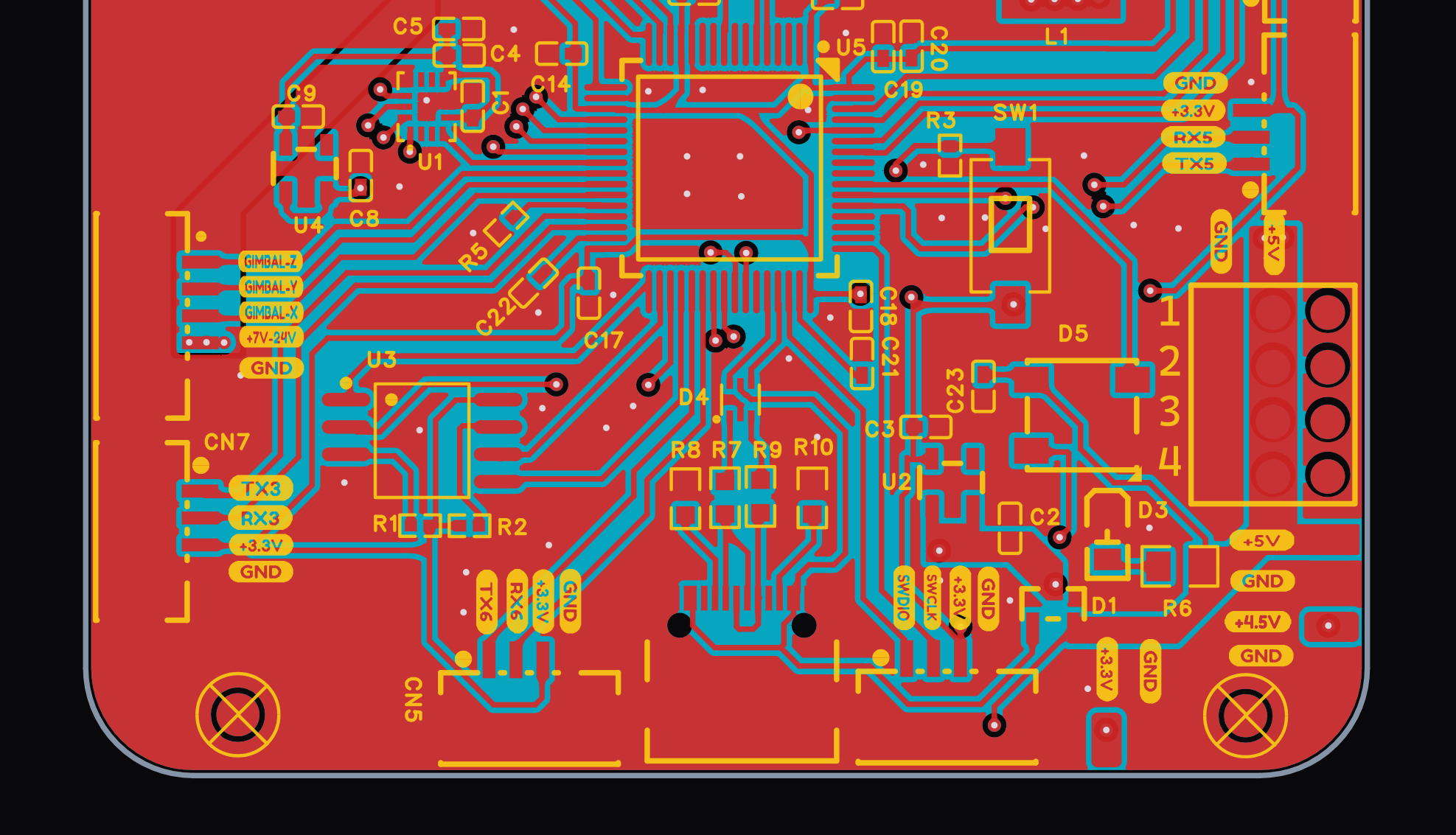
Copper Flood on Signal Layers
A real-world example of copper flood causing more harm than good.
6/23/2026
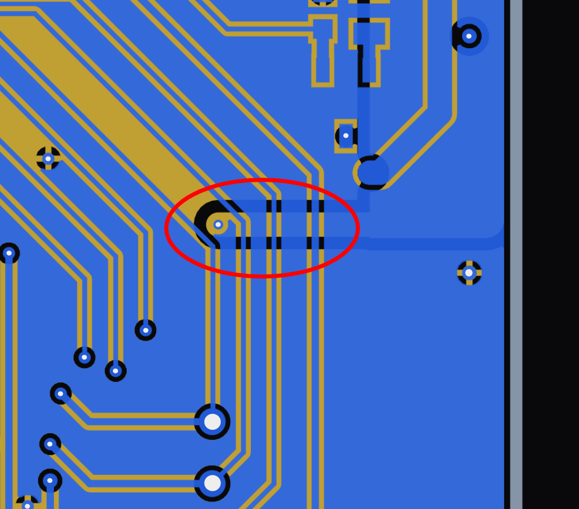
A Simple Fix that Eliminates Risk
How moving traces just a few centimeters can make all the difference in EMC behavior.
6/17/2026
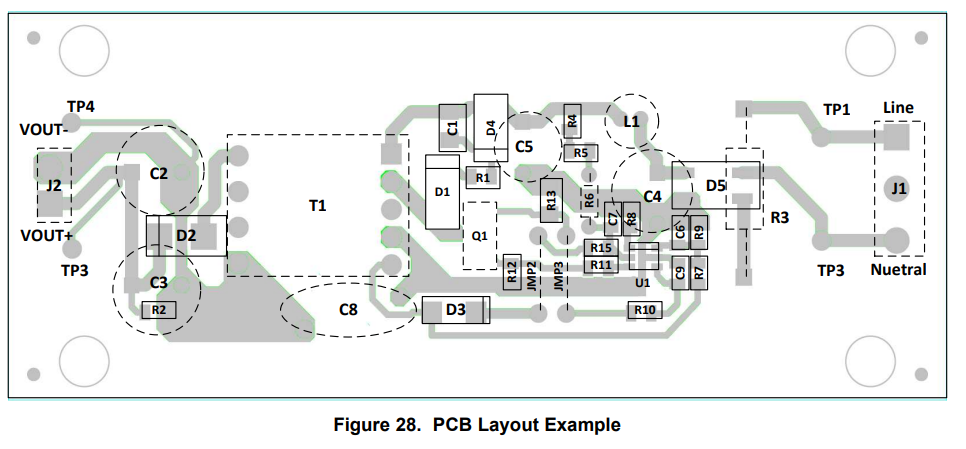
Don't Always Trust the Datasheet
If you use this reference layout in your design, EMC problems are guaranteed.
6/9/2026
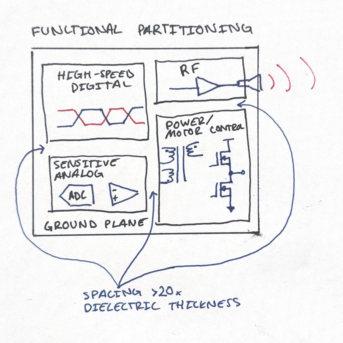
PCB Floor Planning for Low EMI
The physical placement of parts on your PCB is the first line of defense in EMC.
6/2/2026
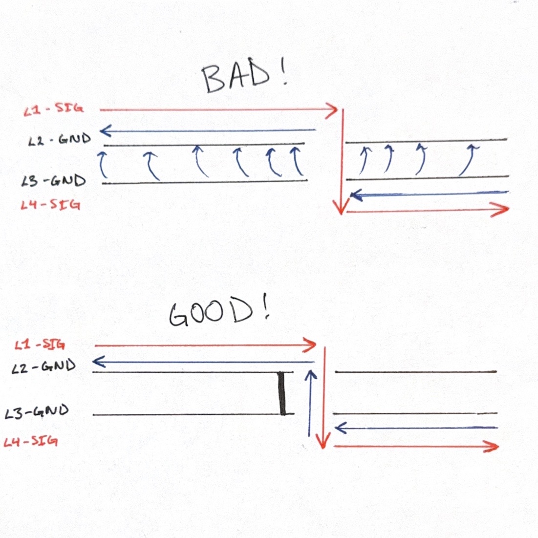
Using Stitching Vias at Layer Transitions in SGGG Boards
Stitching vias are an incredibly useful tool when managing fields at layer transitions in PCBs.
5/26/2026
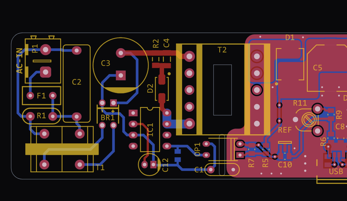
Managing Common-Mode Current in an Offline Converter
Transformer currents between isolated domains are a common source of EMC issues. A simple, properly placed component is cheap insurance.
5/19/2026
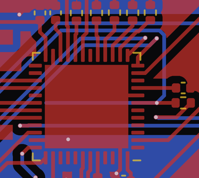
The Importance of a Solid Reference Plane Adjacent to Microcontrollers and Signals
Continuous reference planes are critical for modern microcontrollers and high frequency signals.
5/12/2026