PCB Floor Planning for Low EMI
The physical placement of parts on your PCB is the first line of defense in EMC.
6/2/2026
Placing components on a PCB without strict rules can lead to EMC lab failures. If your design mixes analog, high-speed digital, RF, power conditioning, or any combination of those, functional grouping and physical separation must be considered.
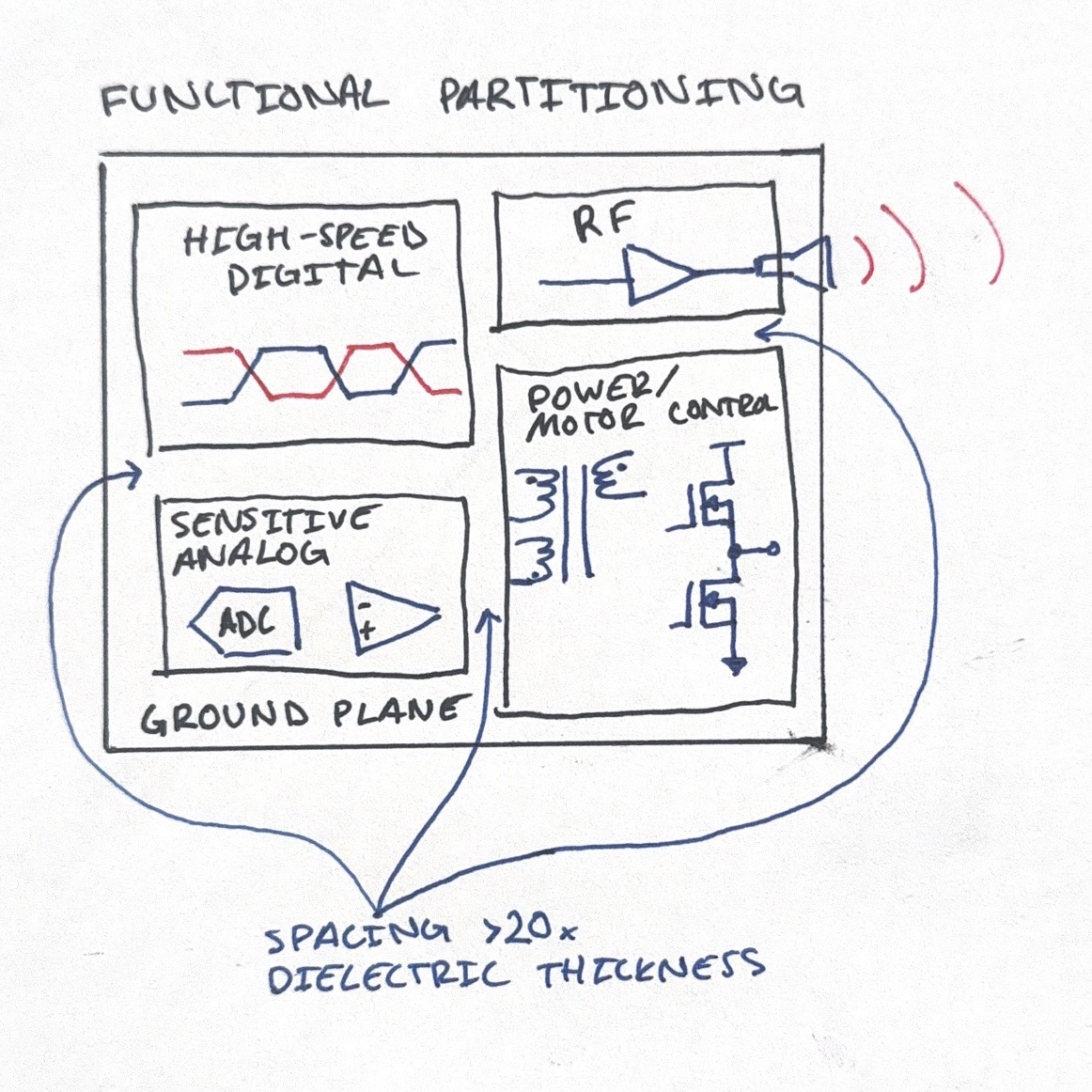
Here is the physics of mixed-signal partitioning:
• Energy Moves in the Dielectric: Energy in a circuit board travels as EM waves in the dielectric between the trace and the return plane. If an aggressor (digital/power) and a victim (analog) share the same dielectric space, their fields can cross-couple.
• Partition by Function & Voltage: Isolate components into dedicated zones (Power, Digital, RF, Analog, etc.). Grouping by functional family and voltage level prevents higher-energy transient fields from overlapping with sensitive circuits.
• Continuous Reference: IC manufacturers' datasheets often tell you to cut your ground planes into AGND and DGND. In modern high-frequency design, this is destructive. If a trace crosses that split, the return current loses its path, and the fields couple to the nearest copper.
• Distance Between Groups: Run a single, solid, continuous ground plane instead. High-frequency return currents naturally follow the path of least inductance, which is directly beneath the trace. Maintain a physical separation between zones equal to or greater than 20x your dielectric thickness as a rule of thumb.
PCB design isn't just about connecting nodes on a schematic; it's about managing fields to ensure products behave as intended.
Need this level of analysis for your next board?
Get in touch with our experts to book a consultation.