Copper Flood on Signal Layers
A real-world example of copper flood causing more harm than good.
6/23/2026
Adding ground copper in every open space isn’t a great rule of thumb.
More ground is not automatically better. If your PCB already has a solid, continuous reference plane, flooding the signal layer with ground copper is usually redundant and possibly detrimental.
Take a look at the top-layer pour in this four-layer layout. It fills the space, but it introduces EMC and signal integrity risks. Notice the solid, continuous reference plane on layer two.
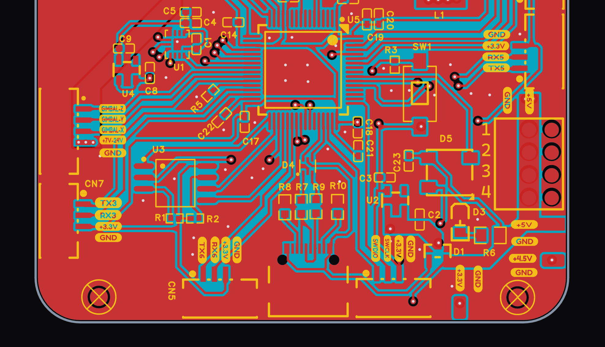
Here is the physics of why a redundant top-layer ground pour can compromise your board:
• Floating Resonators: When copper is poured between traces, it creates isolated islands and long, narrow peninsulas. If these shapes are not securely tied to the main ground plane, they become floating planes that act as resonators, coupling to noise and radiating out into the environment.
• Return Path Disruption: If a high-frequency signal trace routes across a poorly stitched, fragmented ground fill, the return path can become uncontrolled. Crossing multiple split ground fill areas can effectively act like routing over a split in your primary return plane.
• Impedance Discontinuities: Flooding ground copper directly adjacent to high-speed traces alters their fringing capacitance. Because signals reflect whenever the instantaneous impedance changes, this proximity effect alters the characteristic impedance of the trace. This mismatch can cause signal reflections and ringing that generate even more high-frequency harmonic noise.
The solid layer two reference plane is already doing the heavy lifting for your return paths.
The Fix: You should generally avoid filling empty board space with ground return copper, as it often does not help and can sometimes hurt performance. If you don't explicitly need top-layer copper for thermal dissipation or specific shielding, delete it.
If you must keep it, make sure to use plenty of stitching vias to ensure it is equipotential with the main reference plane.
P.S. I do like having some top-layer reference copper underneath microcontrollers for stray fields from the IC to attach to.
Need this level of analysis for your next board?
Get in touch with our experts to book a consultation.