Managing Fields in an SGPS Stackup
How to avoid EMC risks when transitioning between layers with a 4-Layer SGPS PCB.
7/7/2026
Routing high-speed signals from Layer 1 to Layer 4 on a Signal-Ground-Power-Signal stackup introduces a potential compliance risk.
While this routing strategy is generally fine for low-speed logic or GPIOs, using it for high-speed transitions can complicate things.
Take a look at the cross-section in this image to see what the fields are doing inside the board.
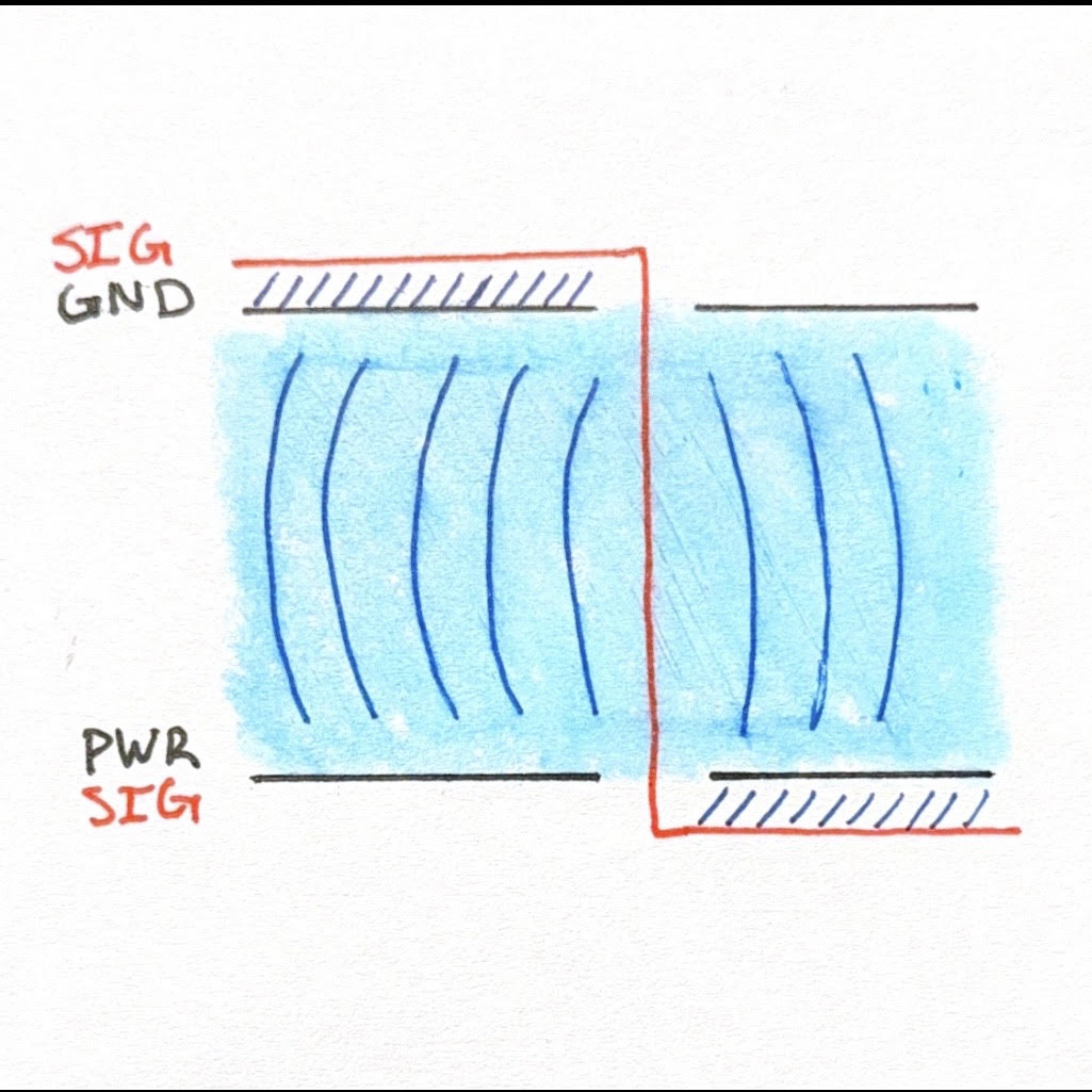
Here’s why an L1-to-L4 high-speed transition requires careful management:
• Where the Fields Live: Circuit energy travels as an electromagnetic wave in the dielectric space, not inside the copper (the red traces and via). Layer 1 signals are bound in the dielectric between L1 and the L2 Ground plane. Layer 4 signals are bound between L4 and the L3 Power plane.
• Power Distribution: The energy for the Power Delivery Network (PDN) travels in the dielectric core (the light blue space) between the L2 Ground and L3 Power planes. This is typically a 30 to 40 mil gap.
• Changing Layers: When a signal drops from L1 to L4, the electromagnetic wave must transfer across the L2-L3 dielectric. Because Power and Ground are at different DC potentials, a simple stitching via cannot be used to provide a direct return path.
• Risk of Mixing: Without a defined, low-impedance return path, the signal's fields (the blue lines) can become unbound and spread throughout the core. At higher frequencies, injecting signal energy directly into the PDN's dielectric space can excite the board to resonate and radiate common-mode noise from the exposed edges of the PCB.
A Band-Aid:
If the layout is almost locked and you are constrained to an SGPS stackup, place stitching capacitors immediately adjacent to the high-speed signal via. This provides a high-frequency AC return path for the displacement current to bridge the gap and contain the fields.
A Better Solution:
For future layouts dealing with high-speed interfaces, consider shifting to a Signal-Ground-Ground-Signal stackup. This structure ensures that every layer transition can be bounded by a stitching via (or two).
Need this level of analysis for your next board?
Get in touch with our experts to book a consultation.