Don't Always Trust the Datasheet
If you use this reference layout in your design, EMC problems are guaranteed.
6/9/2026
We've found that you can't always trust the guidelines in datasheets and application notes. Taking a look at this example from a popular flyback controller's datasheet, it should be easy to see why.
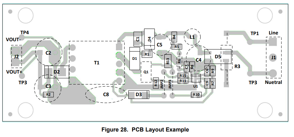
Any product that uses a layout inspired by this reference design would be an emissions nightmare. Here is what they should have done:
• If forced to use a single layer: There must be adjacent copper with a low-impedance connection to the reference node (like a strategic ground pour on Layer 1).
• If moving to a two-layer board: There must be separate, localized ground pours underneath the primary and secondary circuits with proper clearance. (Never route a continuous copper plane across the isolation gap).
• Bridge the gap: Since the Y-capacitor is already included, it must bridge these two localized ground planes with the tightest possible routing to effectively shunt common-mode currents back to their source.
• Minimize the antennas: Tighten up the gate drive, switching, and snubber loops, and shrink the switch-node copper area to the absolute minimum to reduce electric field radiation.
Need this level of analysis for your next board?
Get in touch with our experts to book a consultation.