A Simple Fix that Eliminates Risk
How moving traces just a few centimeters can make all the difference in EMC behavior.
6/17/2026
Sometimes avoiding an EMC risk doesn't require adding components or changing your stackup.
Take a look at this layout snippet from a recent review. These blue traces on layer 4 are routed right over a void in the gold layer 3 reference copper.
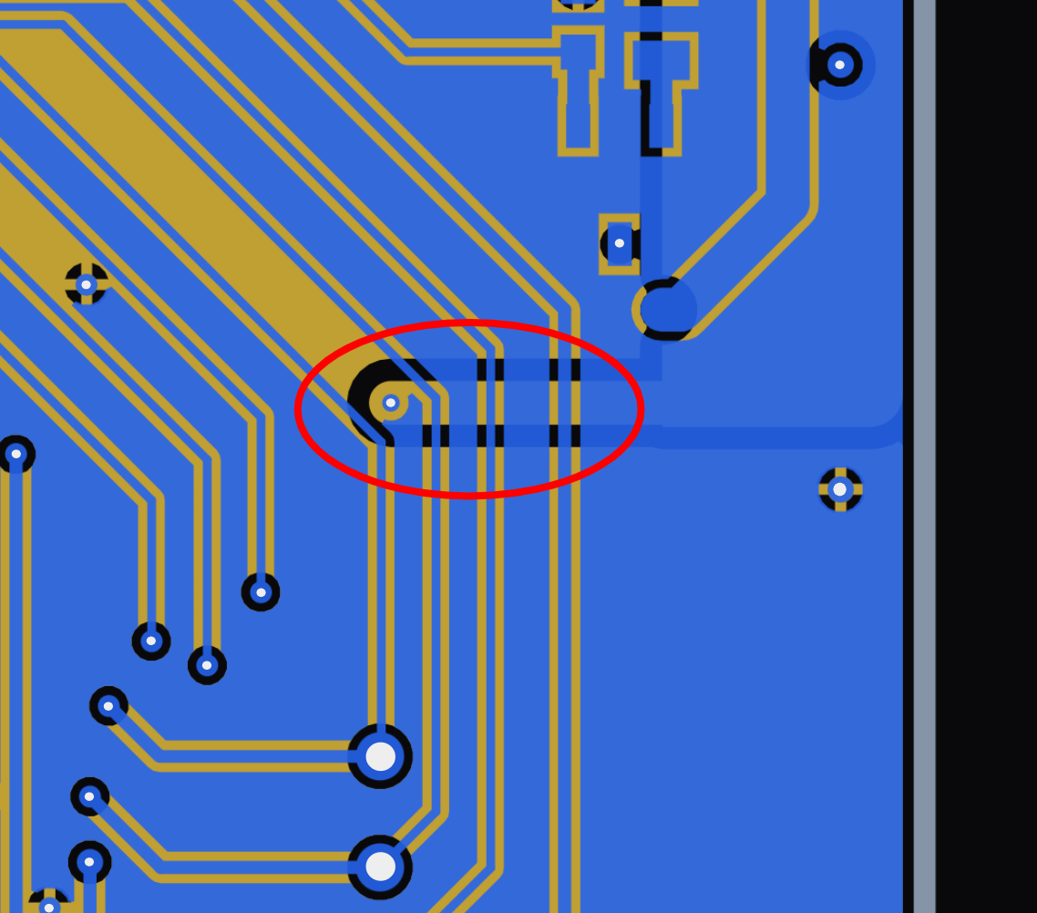
Here is the physics of this risk:
• The Return Path: High-frequency current always seeks the path of least impedance back to the source. When the adjacent reference plane disappears, the return current is forced to detour around the void, increasing the loop area.
• Unbounded Fields: Without a continuous reference plane directly beneath the traces, the electromagnetic fields are no longer tightly bound to the board. They will spread into the dielectric and increase the emissions signature of the board, especially since the void in the reference plane continues to the board edge.
The fix here is completely free, as long as it’s caught at the right time.
Simply move these four signals to the left so they sit securely over the solid copper reference region. It’s not shown in this image, but moving the via that connects the copper island on layer 3 actually improves the layout of the top layer circuit it’s connected to.
Need this level of analysis for your next board?
Get in touch with our experts to book a consultation.